Design rules for capacitive touch sensors

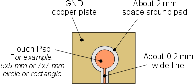
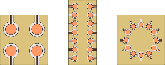
Recommended touch pattern layout
To obtain best results, following design rules should be considered:
- Touch pad size is limited by allowed input capacitance
- Space around touch pad and GND plane should be about 1-2 mm
- Adjacent touch pads should be separated by GND plane
- Connection lines should be only about 0.2 mm wide
- Wire between pad and device input should be as short as possible
- Another wires should be kept out of pad layout
- Touch pad opposite or inner layer should be empty (no GND filling, since it lower sensitivity)
- For multi-channel devices a distance between pads, pad and another pad wire and between input wires should be kept
- Low impedance PCB design is recommended
- Front panel should be based on non-conductive materials with low εr like ABS, glass, plexiglass, etc.

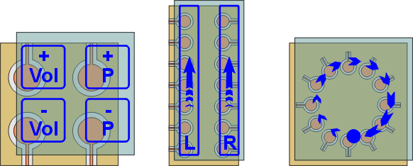
Pads created on PCB (single buttons, scrolling slider, wheel slider)

Touch pads can be covered by dielectrical material with printing
(non-conductive foils, ABS instrument case, glass, plexiglass, etc.)
For more application circuits and component explanation see detail documentation available on our web.
How_to_buy (touchSEMI - Simple way to your favorite devices)
Application_fields (Applications of Capacitive Touch Sensors, Modules and Comparators)
Simple_circuits (Basic wiring diagrams of capacitive touch sensors)
Design_rules (Design rules for capacitive touch sensors)
Touch_sensors (Capacitive touch sensors, Capacitive sensor modules, Capacitance comparator)
Info (touchSEMI - Capacitive touch and proximity sensors)
Theory_of_operation (Principle of capacitive touch sensors)
|